Technologies, devices and circuits, assemblies and modules

Technologies

We offer epitaxy structures on wafers up to 4'' or 8'' as well as process lines on wafers up to 4'' according to application specifications.

Lateral

  • AlGaN/GaN-on-Si (N-OFF, N-ON, 48 V, 650 V, 1200 V)
  • AlScN/GaN-on-Si
  • GaN-on-CMOS hetero-integration (micro-transfer printing [µTP], Wafer-to-Wafer, Si-substrate removal etc.)
  • GaN-on-X (X = GaN, SiC, QST®, sapphire, diamond) 
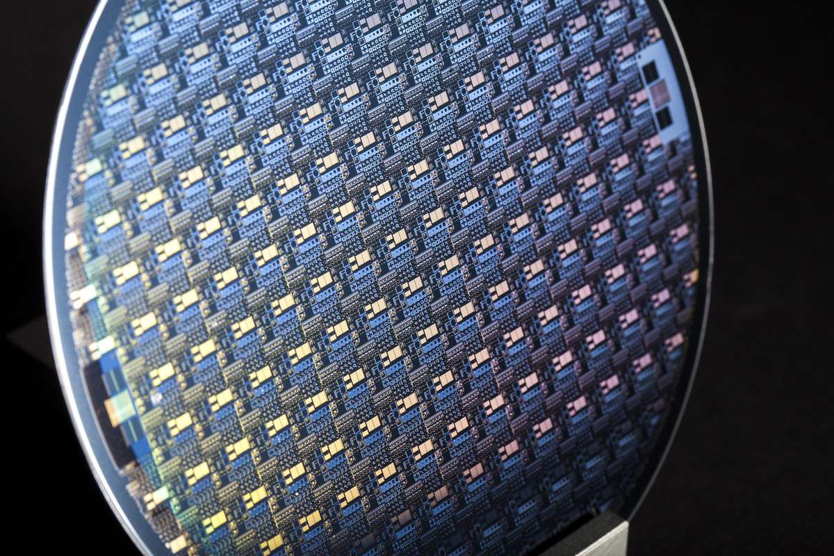
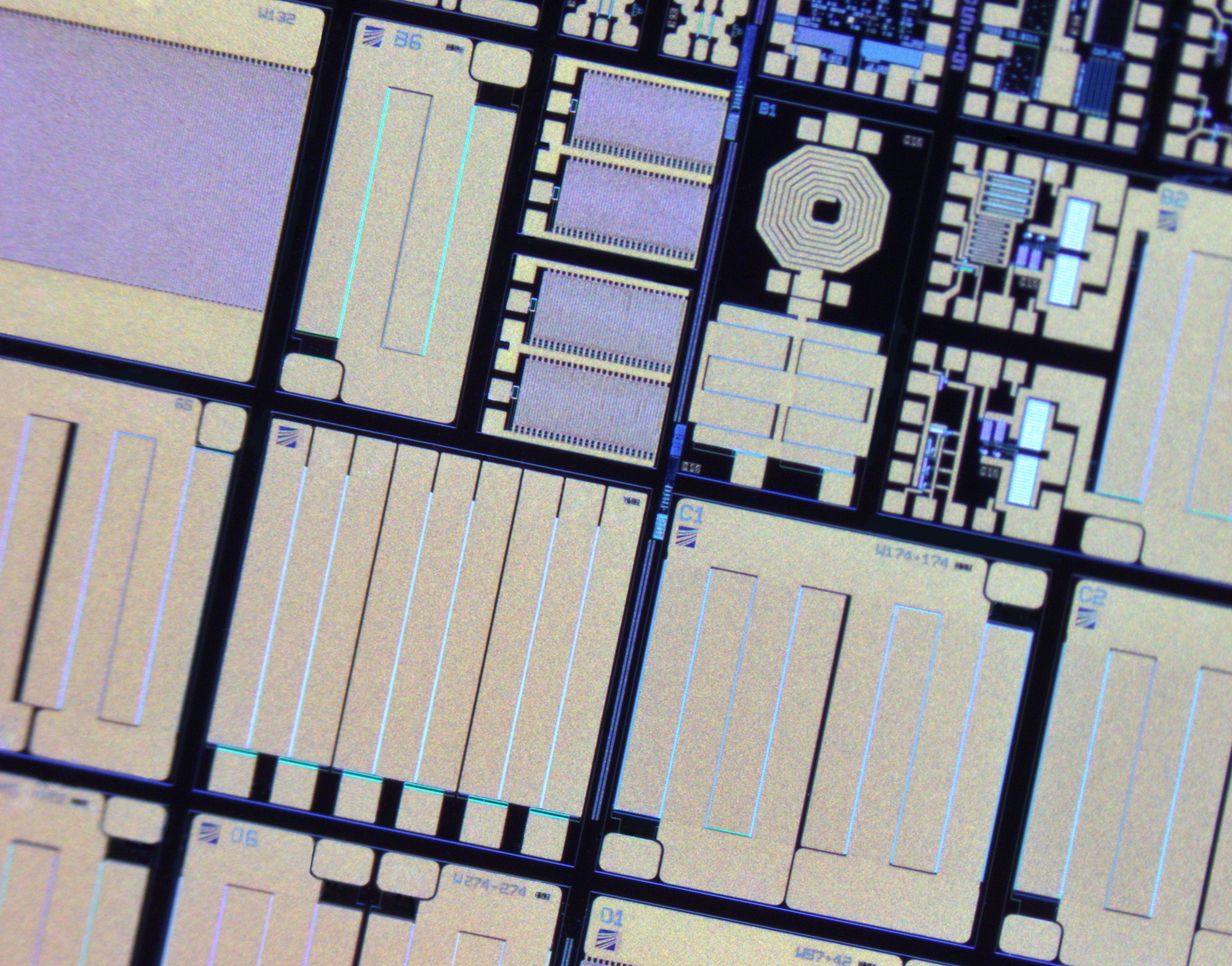
Processed epitaxial wafer of SiC-GaN, made by Fraunhofer IAF
© Fraunhofer IAF
Epitaxy wafer with quasi-vertical GaN-on-SiC process

Vertical and quasi-vertical

  • GaN-on-GaN (vertical)
  • GaN-on-Si (quasi-vertical)
  • GaN-on-Sapphire (quasi-vertical)
  • GaN-on-SiC (quasi-vertical)
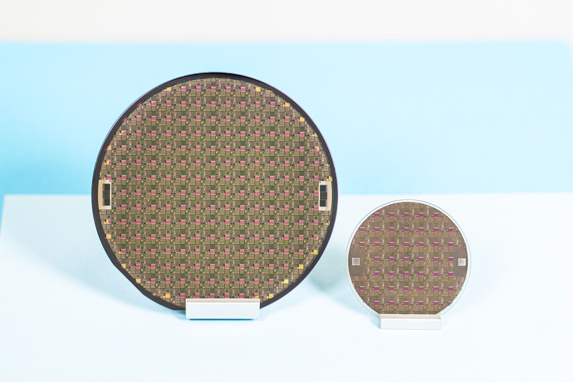
Two epitaxial wafers (2'' and 4'') with vertical GaN-on-GaN process developed at Fraunhofer IAF
© Fraunhofer IAF
Epitaxial wafers (2'' and 4'') with vertical GaN-on-GaN process

Devices and ICs

With know-how and a unique research infrastructure, we develop integrated and monolithic integrated circuits and devices based on power semiconductors such as GaN. For example, we realize 1200 V components based on GaN for inverters in traction drives for electric cars.

Lateral devices

  • HEMTs (N-OFF, N-ON, MIS | 48 V, 200 V, 650 V, 1200 V)
  • HEMT with intrinsic free-wheeling diode
  • High voltage cascodes
  • Diodes (lateral field rectifier, Schottky diodes)

GaN power ICs

  • Gate driver (multi-stage approaches, bootstrap ICs)
  • Monolithic half-bridges (3-phase inverter IC)
  • Current sensors (senseFET, quasi-shunt) and temperature sensors
  • Protection circuits
  • Control logic (PWM generator, amplifier, comparator)
GaN-on-Si multiwafer by Fraunhofer IAF
© Fraunhofer IAF
GaN-on-Si chip designs enable efficient and compact devices that are required for low voltage applications, for example.

All-in-GaN power ICs

  • Monolithic point-of-load converter
  • Active GaN diode IC

Vertical devices

  • Diodes
  • CAVETs and co-integrated HEMTs
  • FinFETs
  • MOSFETs (process development)
  • JFETs and selective overgrown HEMTs (new approach for vertical GaN power ICs)
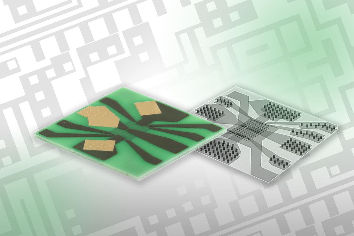
Monolithic half bridge with low voltage HEMT for point-of-load converter realized by PCB embedding; developed at Fraunhofer IAF
© Fraunhofer IAF
Researchers at Fraunhofer IAF have used PCB embedding to realize a monolithic half bridge with low voltage HEMT for a novel point-of-load converter.

Assemblies and modules

We use hetero-integration and compact assembly and connection technology to create compact high-performance modules.

Die attach

  • Solder (AuSn 80/20)
  • Sinterpaste
  • Adhesives (conductive, non-conductive)

Wire bonding

  • Gold, copper
  • Ball-wedge, wedge-wedge
  • 25 µm, 50 µm etc.

PCB embedding

  • Extern partner
  • Si-removal (freestanding, GaN-on-PCB)
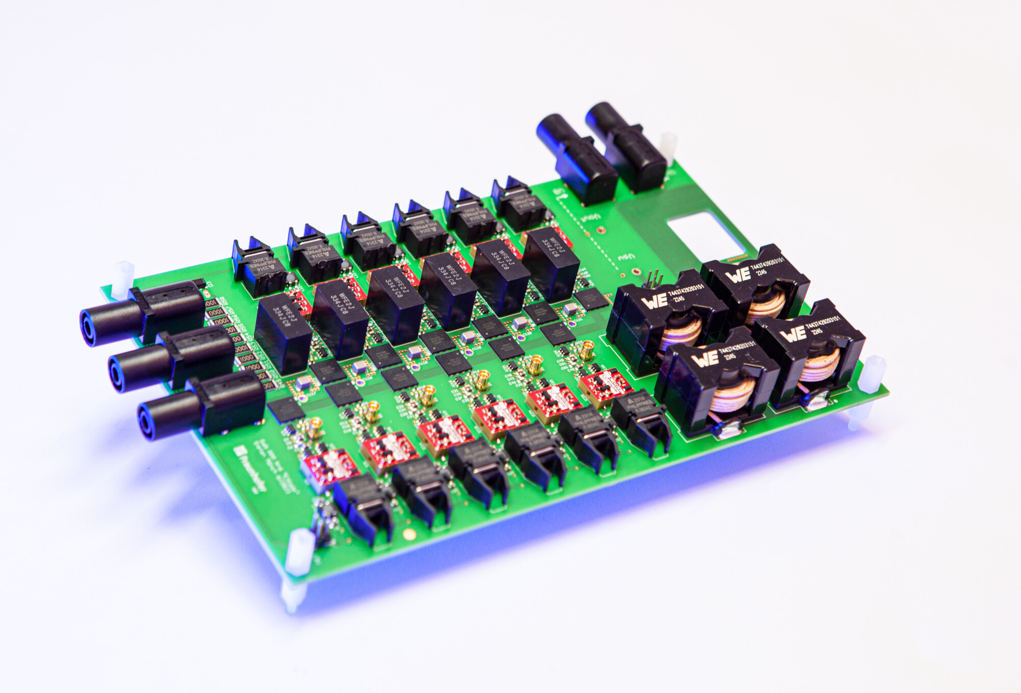
48 V/5 kW motor inverter with GaN-based three-phase half bridge, developed at Fraunhofer IAF
© Fraunhofer IAF
48 V/5 kW motor inverter with a GaN-based 3-phase half bridge

Packages for devices

  • TO engineering types
  • Quad flat no leads package (QFN)
  • DFN8 PCB
  • Dual-in-line for logic
  • Flip chip (solder jetting)

Module manufacturing

  • DCBs (AlN etc. | laser-structured, prototyping)
Multilevel voltage converter with high-voltage GaN transistors, developed at Fraunhofer IAF
© Fraunhofer IAF
Multilevel voltage converter with high-voltage GaN transistors

Range of services in GaN power electronics

Research and development services along the semiconductor value chain

Epitaxy

Order epitaxial layers from us according to your specifications for electronic and optoelectronic components.

Wafer runs

We offer multi-project wafer runs (MPW) and complete mask processing for electronic and optoelectronic components with frontside and backside processing.

Analysis of semiconductor materials

We offer analytical methods for the chemical and structural characterization of bulk semiconductors, heterostructures and thin-film systems.


Devices, ICs, modules

We develop innovative devices, ICs, and modules with world-class performance and efficiency.

Metrology

Fraunhofer IAF has a large number of measurement systems for characterizing ICs and modules.


Semiconductor value chain

We offer customized R&D services along the semiconductor value chain.


Questions, advice, collaboration

Receive specific information on your subject area and get personal advice. Collaborate with us in a project or commission us.