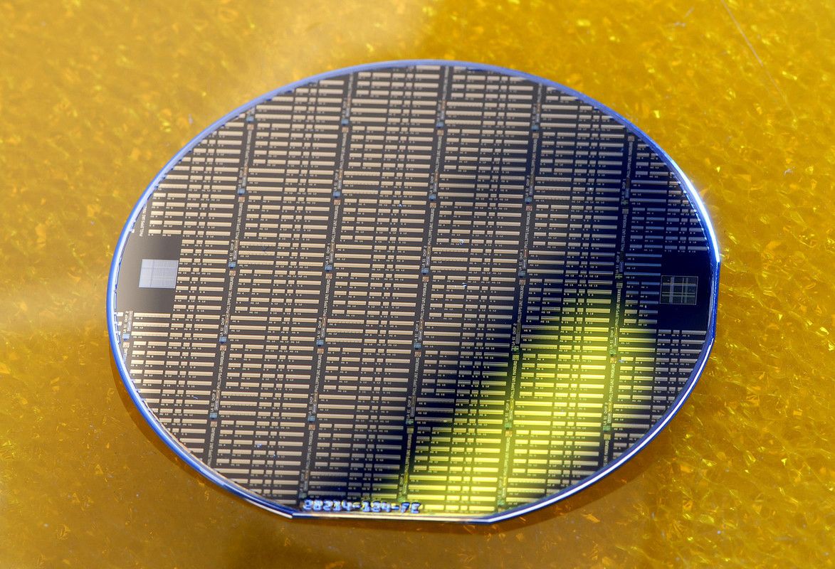
Multi-Project Wafer Runs

Wafer Runs for transistors, integrated circuits (ICs) as well as electronic and optoelectronic devices


Based on its epitaxial and technological capabilities, Fraunhofer IAF offers (multi-project) wafer runs (MPW), entire mask processing and the realization of electronic and optoelectronic devices for external customers. Both frontside and backside processing is possible. The runs are offered regularly every four to six months.  

Fraunhofer IAF has a state-of-the-art clean room for processing of cutting-edge III-V semiconductor devices with e-beam, optical stepper, and laser lithography as well as deposition and etching of various dielectrics and metals. In order to maintain and expand its excellent processing capabilities, Fraunhofer IAF invests in new equipment every year.

Technology services in high-frequency and power electronics

InGaAs HEMT technologies

  • 50-35-20 nm InGaAs metamorphic HEMT (mHEMT)
  • mHEMT-on-Insulator technology (under development)
  • Design, fabrication, characterization and assembly of monolithic microwave integrated circuits (MMICs) for frequencies up to 700 GHz
  • State-of-the-art noise figure performance
  • Extremely high bandwidth
  • Multifunctional MMICs
  • On-chip broadband antennas
  • Performance enhancement with cryogenic operation


GaN-on-SiC technologies

  • Fabrication of HEMT devices from 0.5 μm down to 50 nm gate length
  • Highest output power
  • Frequency range up to 200 GHz
  • Highest power conversion efficiency
  • Proven reliability and robustness
  • Integrated passive devices


GaN-on-Si technologies

  • GaN-based power ICs
  • Half-bridges, gate drivers
  • On-chip sensors


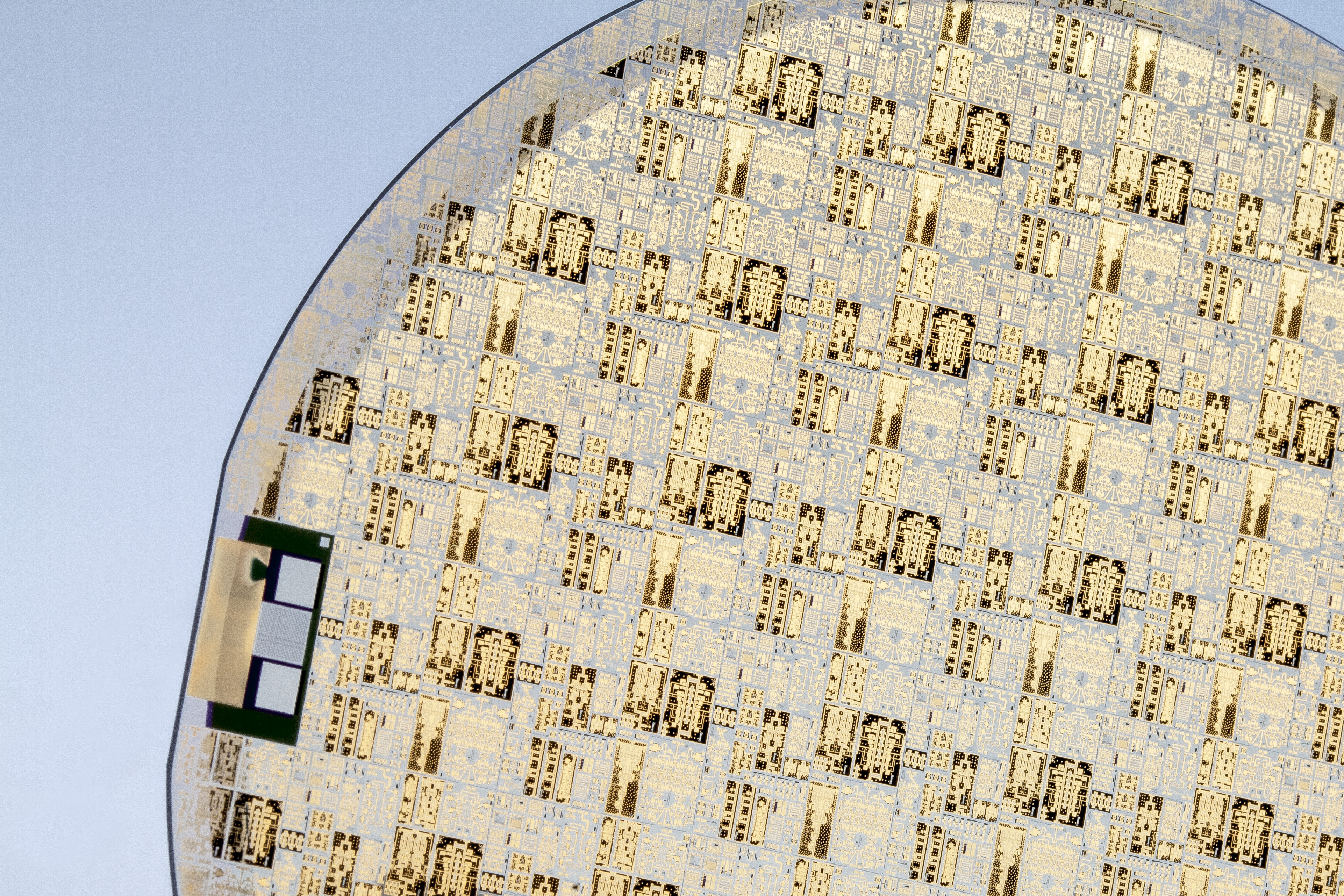
Processed GaN on SiC wafer.
© Fraunhofer IAF
Processed GaN-on-SiC wafer
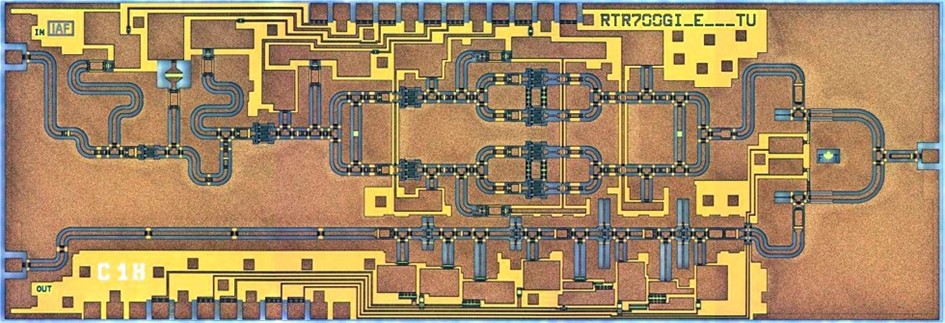
Transceiver MMIC of Fraunhofer IAF integrating power amplifier, switch and low-noise amplifier
© Fraunhofer IAF
Transceiver MMIC integrating power amplifier, switch and low-noise amplifier
Low-noise amplifier (mHEMT – 50 nm).
© Fraunhofer IAF
Low-noise amplifier (mHEMT – 50 nm)

Technology services in optoelectronics

GaAs and Inp based lasers

  • Double trench or buried het processing
    • Broad area lasers
    • Ridge-waveguide lasers
    • Tapered lasers and amplifiers
  • Customized faced coating (NIR/IR) including characterization


IR and UV photodetector technologies

  • Mono- and bispectral detectors from MWIR (3–5 µm) up to LWIR (8–12 µm), with InAs/GaSb or InAs/InAsSb T2SL
  • Single-photon avalanche diodes (SPADs) based on InGaAs/InP
  • UV-C detector matrices in the solar-blind range below 280 nm with AlGaN


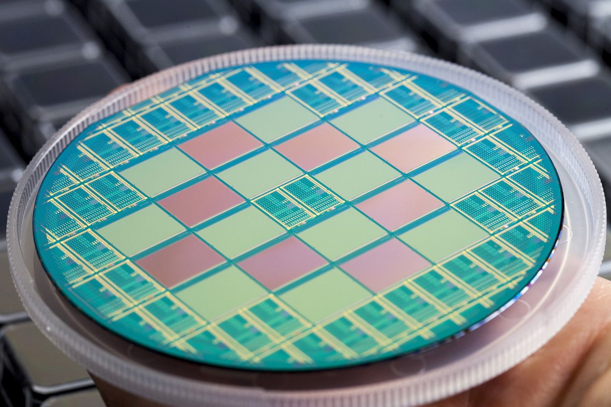
Wafer of Fraunhofer IAF caontaining detectors for short-wavelength infrared
© Fraunhofer IAF
3-inch InGaAs/InP wafer comprising APD arrays and single-element devices for use at 1550 nm wavelength
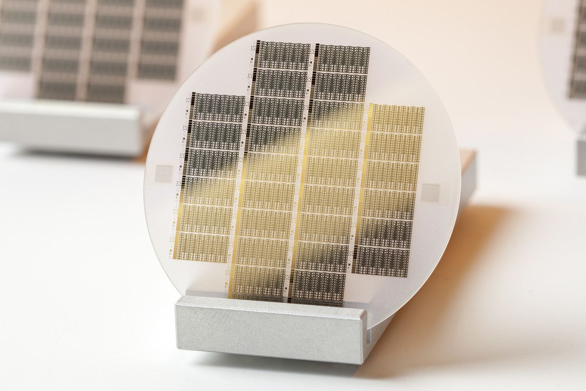
Wafer of Fraunhofer IAF containing UV detectors
© Fraunhofer IAF
UV detectors on sapphire substrate
Wafer of Fraunhofer IAF containing lasers on silicon substrate
© Fraunhofer IAF
Low-noise amplifier (mHEMT - 50 nm lowest power)