»We hope that at best we can revolutionize the assembly technology«

Researcher Christian Zech talks about his patent application for a novel assembly technology for high frequency systems

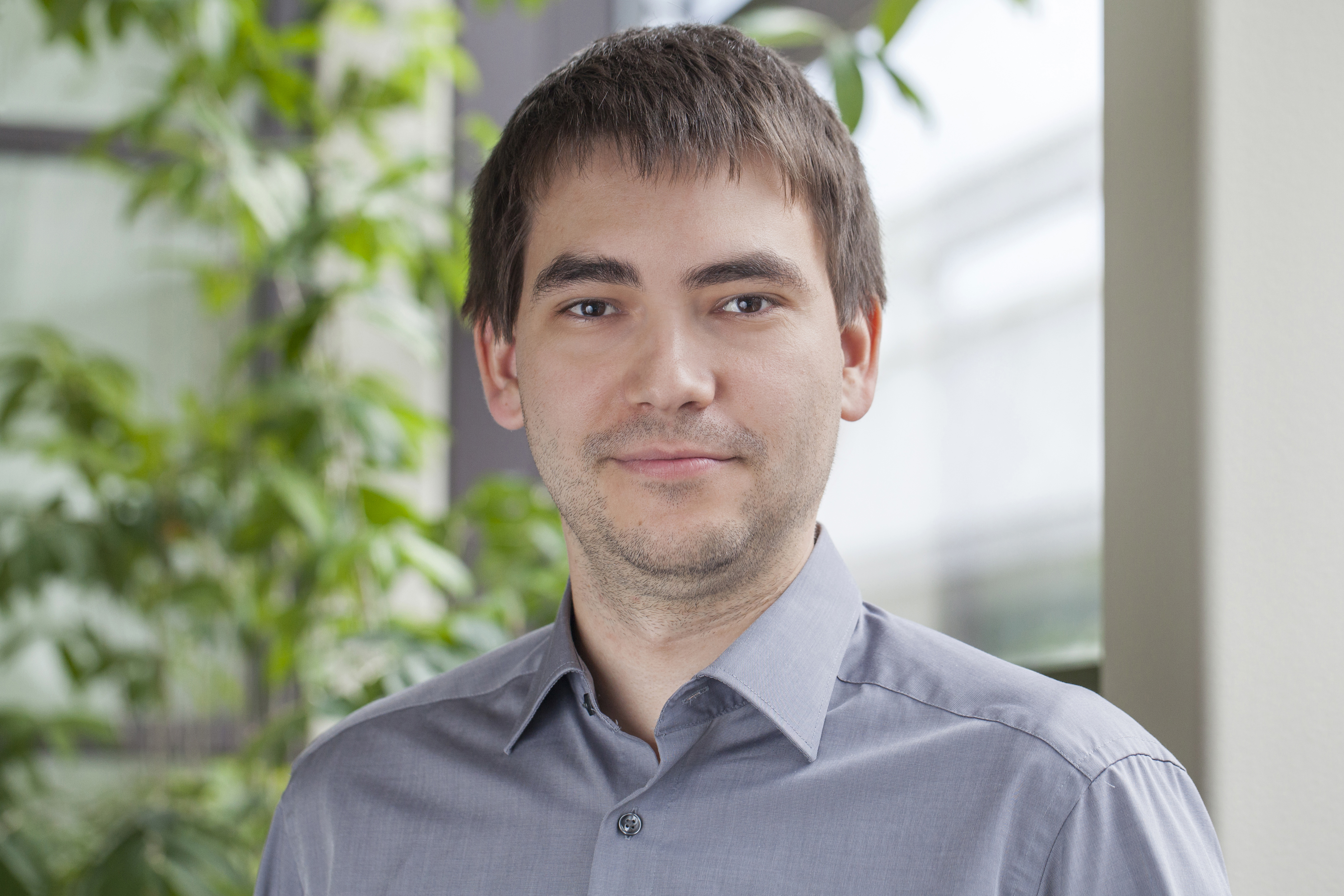
Christian Zech is writing his dissertation in the field of high frequency electronics.
© Fraunhofer IAF
Christian Zech is writing his dissertation in the field of high frequency electronics.
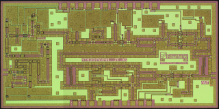
Die benötigten monolithisch integrierten Mikrowellenschaltungen (MMICs, engl. monolithic microwave integrated circuits) zur Realisierung der Hochfrequenzkomponenten, werden in der metamorphen High-Electron-Mobility-Transistor (mHEMT)-Technologie des Fraunhofer IAF gefertigt.
© Fraunhofer IAF
Die benötigten monolithisch integrierten Mikrowellenschaltungen (MMICs, engl. monolithic microwave integrated circuits) zur Realisierung der Hochfrequenzkomponenten, werden in der metamorphen High-Electron-Mobility-Transistor (mHEMT)-Technologie des Fraunhofer IAF gefertigt.
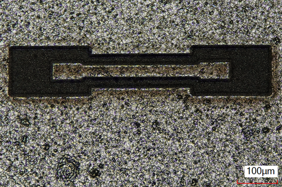
Lasered structrue in silver ink.
© Fraunhofer IKTS
Lasered structrue in silver ink.

Your patent is called »Multilayer ceramic assembly technology for high-frequency systems«. What does that mean?

In the past, our modules for radar and communication applications were manufactured in a complex and expensive way using waveguide technology. Each module has to be precisely milled individually in complex work. This is why we have been using printed circuit boards for several years that are inexpensive and easy to manufacture. These work very well up to 100 GHz. At higher frequencies, however, the performance drops dramatically. There was no alternative to waveguides – until now. 

»With multilayer ceramics, so-called low temperature cofired ceramics LTCC, we can realize high-frequency systems similar to printed circuit boards at lower cost, which work up to over 300 GHz. Everyone today talks about communication applications such as 5G and 6G, which use high frequencies, but how such systems can be built cost-effectively is not yet clear. Our technology could be the solution. We hope that at best we can revolutionize the assembly technology.«


How does this new assembly technology work in comparison to the previous one?

A printed circuit board consists of a substrate, typically a fiberglass-reinforced plastic. For high frequencies, on the other hand, special liquid crystal polymer substrates are used. Here, copper is applied on both sides and structured, i.e. the parts that are not needed are etched away. The components are then applied.

»The structure on a ceramic board works very similarly. You start with a wafer-thin layer of LTCC. However, instead of etching the copper surfaces, silver ink is printed by aerosol jet printing. The great thing is that very fine structures can be applied with this technique. Finer than they could be etched today with copper and finer than they could be produced with another printing process.«

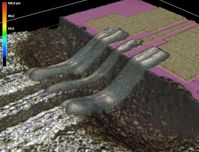
Another huge advantage is that bond processes are no longer necessary. Previously, the chip was inserted on the circuit board and then contacted with bonding wires. This is technically very complex and also leads to losses starting at around 100 GHz being so high that the system is no longer efficient. Our idea now is that the chip is located in the ceramic and the printer then prints the conductor paths on the ceramic. It does not stop at the chip, but simply prints over it – so the silver ink automatically establishes the contact. We are developing this method further in the »TeraKer«  project.

Aerosol jet printed wires with direct contact to the chip.
© Fraunhofer IKTS
Aerosol jet printed wires with direct contact to the chip.

What effects do you hope your patent will have?

So far there has been the chicken and egg problem. The high frequencies are not used because the systems are expensive, and because demand is low, they do not become cheaper. The use of 77 GHz for automotive radars has only become established because the circuit boards can be produced cheaply. There is no need for special production lines.

»If we can transfer that to the high frequencies, we might be able to trigger a technology push. There are already commercial ceramic manufacturers who have experience in the 2 –  4 GHz range for wireless communication applications, so we hope to make this production also possible for 300 GHz.«


The patent was developed jointly with Fraunhofer IKTS. How did this come about?

At a trade fair at the Fraunhofer joint stand, we got into conversation with colleagues from the Fraunhofer Institute for Ceramic Technologies and Systems (IKTS). They produce ceramic circuit boards. We then tried out whether this technology enabled high powers at higher frequencies - and it does, even at over 300 GHz. IKTS has great expertise in the manufacture of multilayer ceramic substrates and printing techniques, and we contribute our experience in high frequency technology.


------------------------------------------------------------------------

Christian Zech is writing his dissertation in the field of high frequency electronics.

More Information


Interested in starting a career at IAF?

Find all info on jobs and our vacanies here.


Project »TeraKer«

In the »TeraKer« project, Christian Zech and Fraunhofer IKTS are further developing the innovative assembly technology.


Current projects

Find all our current projects in the field of high frequency electronics here.