New machines for future devices
10/08/2020 – Fraunhofer IAF upgrades its equipment for the production of nanostructures and its competence in material analysis with two new machines


“With this state-of-the-art equipment, we are expanding the technological infrastructure at Fraunhofer IAF and thus add to the FMD’s competences for research and development of innovative solutions in high-frequency and power electronics. The e-beam opens up new possibilities, one being the development of innovative devices for quantum computers,” explains Dr. Wolfgang Bronner, Head of Technology at Fraunhofer IAF.
State-of-the-art e-beam enables novel nanocomponents
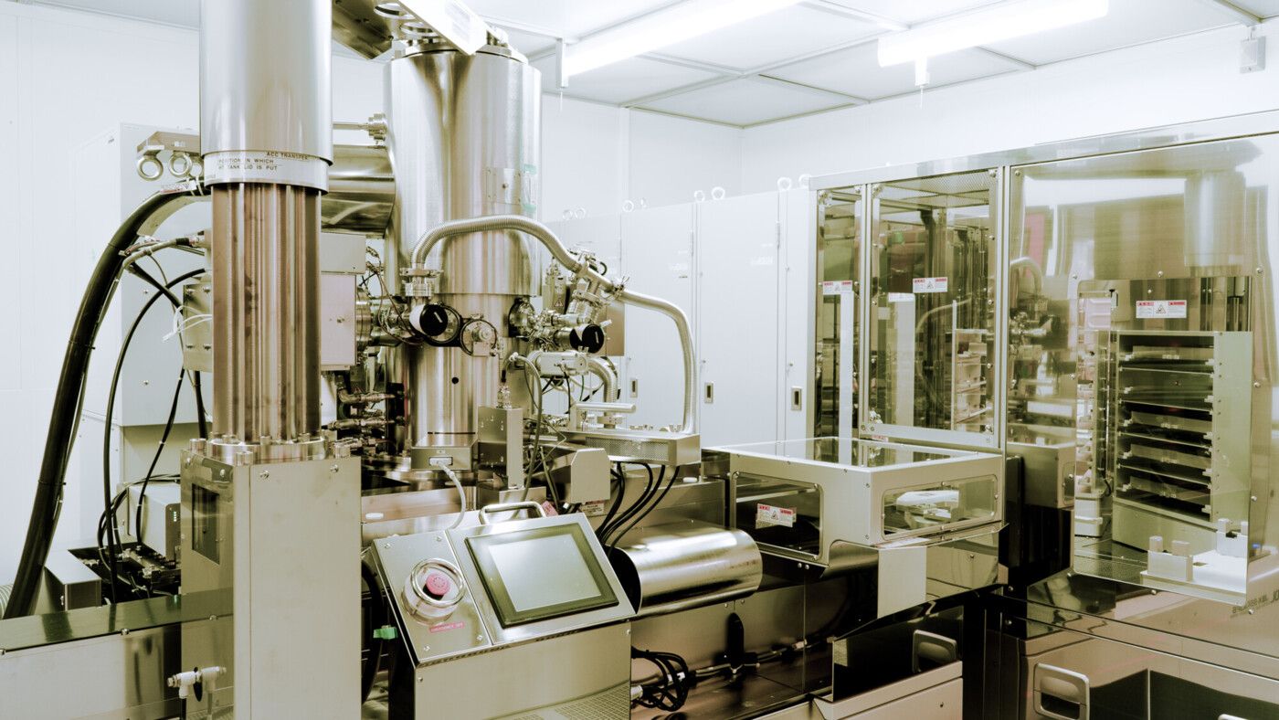
The newly installed e-beam is extremely precise and fast. It allows for shorter process times and smaller structures with significantly higher positioning precision compared to its predecessor model. The electron beam lithography system can produce structures smaller than 10 nm with an accuracy of less than 10 nm in a coating layer. Nanostructures are a prerequisite both for the further development of existing devices and for the realization of new ones. The new e-beam at Fraunhofer IAF is used for the production of very fast switching InGaAs transistors with only 10 nm gate length as well as the development of superconductive nano lattices for quantum processors.
New TOF-SIMS for faster and better measurements
With the new time-of-flight secondary ion mass spectrometer (TOF-SIMS), Fraunhofer IAF now has, in addition to their dynamic SIMS, a further SIMS system for the chemical analysis of bulk semiconductors, semiconductor layers and other materials. At Fraunhofer IAF, they are mainly used for the measurement of wafers with epitaxial layers and processed semiconductor chips, both internally in research, development and quality assurance as well as for external customers.
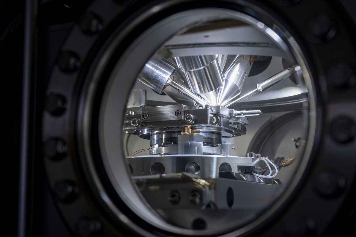
The new TOF-SIMS customized for Fraunhofer IAF is characterized by a higher mass resolution. The system is suited for surface analysis as well as for measurements in greater depth, since in addition to a bismuth ion beam for excitation, a ceasium or oxygen ion beam can also be used to remove material at great depth. The integrated tunneling microscope allows to measure structured or rough surfaces, for example of processed semiconductor chips. A particular strength of the new SIMS is the ability to simultaneously measure mass and depth profiles of a sample. In addition, Fraunhofer IAF is now able to analyze larger wafers of up to 300 mm in diameter; previously, only 100 mm were possible.
Research Fab Microelectronics Germany
Both machines are funded within the framework of the “Research Fab Microelectronics Germany” (FMD). The FMD is a cross-site cooperation of eleven Fraunhofer and two Leibniz Institutes in the field of micro- and nanoelectronics research and development. The idea behind it: A one-stop-shop for R&D services, application solutions and new technologies with a high technology readiness level for a wide range of industrial customers.
The project on which this publication is based was funded by the Federal Ministry of Education and Research under the funding codes 16FMD01K, 16FMD02 and 16FMD03.
 Fraunhofer Institute for Applied Solid State Physics IAF