A new angle on surface acoustic wave filters

In conversation with the PhD students Anli Ding and Niclas Feil

In this interview, PhD students Anli Ding and Niclas Feil talk about their collaboration on a patent for surface acoustic wave resonators based on aluminum scandium nitride (AlScN), which they applied for in 2020.


You are both doing research on the semiconductor material aluminum scandium nitride (AlScN), how did you join IAF/INATECH and get involved in this topic?

Anli — Sometimes, I am surprised myself that I got into applied physics at Fraunhofer IAF, since I started with a bachelor’s degree in material studies in China. Back then, I heard about the degree program Microsystem Engineering at the University of Freiburg. Its good reputation and close contact to industry convinced me to move to Germany for my master’s degree. Thanks to the close collaboration between University and Fraunhofer, I got the opportunity to write my thesis at Fraunhofer IAF and afterwards I got the offer to do my dissertation on AlScN, which I gladly took.

Niclas — Right from the start of my studies, I was particularly interested in crystallography. Piezoelectric acoustic waves are an exciting area of research in which the elastic and piezoelectric properties of crystals are used to describe, for example, surface waves on a crystal surface, similar to those on a water surface. I came across the topic of AlScN during a lecture on compound semiconductors given by Professor Oliver Ambacher. That’s where I first learned about the material and it immediately caught my attention. After the lecture, I directly asked if it was possible to do research in this area. This way I came to my master’s thesis and now also my doctorate at the Department of Sustainable Systems Engineering INATECH, where Professor Ambacher teaches.


What are surface acoustic wave filters based on AlScN and what are the advantages and challenges of the material?

Niclas — The basic material aluminum nitride (AlN) has been known for a relatively long time. It is used, for example, in mobile communications, in so-called bulk acoustic resonators. Essentially, it depends on the crystal structure of the atoms; in the case of AlN, these crystallize in the so-called wurtzite structure. Due to the atomic arrangements of the structure, the crystal has a polarization, which means that it is a pyroelectric, and thus also piezoelectric crystal. This is related to an important property: the electromechanical coupling. It essentially defines the bandwidth of a piezoacoustic filter.

If scandium is added by partially replacing the Al atoms with Sc, the piezoelectric effect is greatly increased by deformation of the crystal lattice, especially for the c-axis of the crystal. To realize these properties, which are already used in bulk filters, for surface acoustic wave (SAWs) based applications, is the idea behind our research.

Anli — Fraunhofer IAF has many years of experience researching AlScN. We could already grow AlScN with good crystal quality and high scandium concentrations in previous research projects. However, we previously only grew c-plane AlScN, which means that the piezoelectric axis is perpendicular to the substrate. This allows for high performance bulk acoustic resonators, but not for SAWs. So we had to find a way to tilt the c-axis of the AlScN about 90° to capitalize on the great potential of AlScN for SAW resonators.

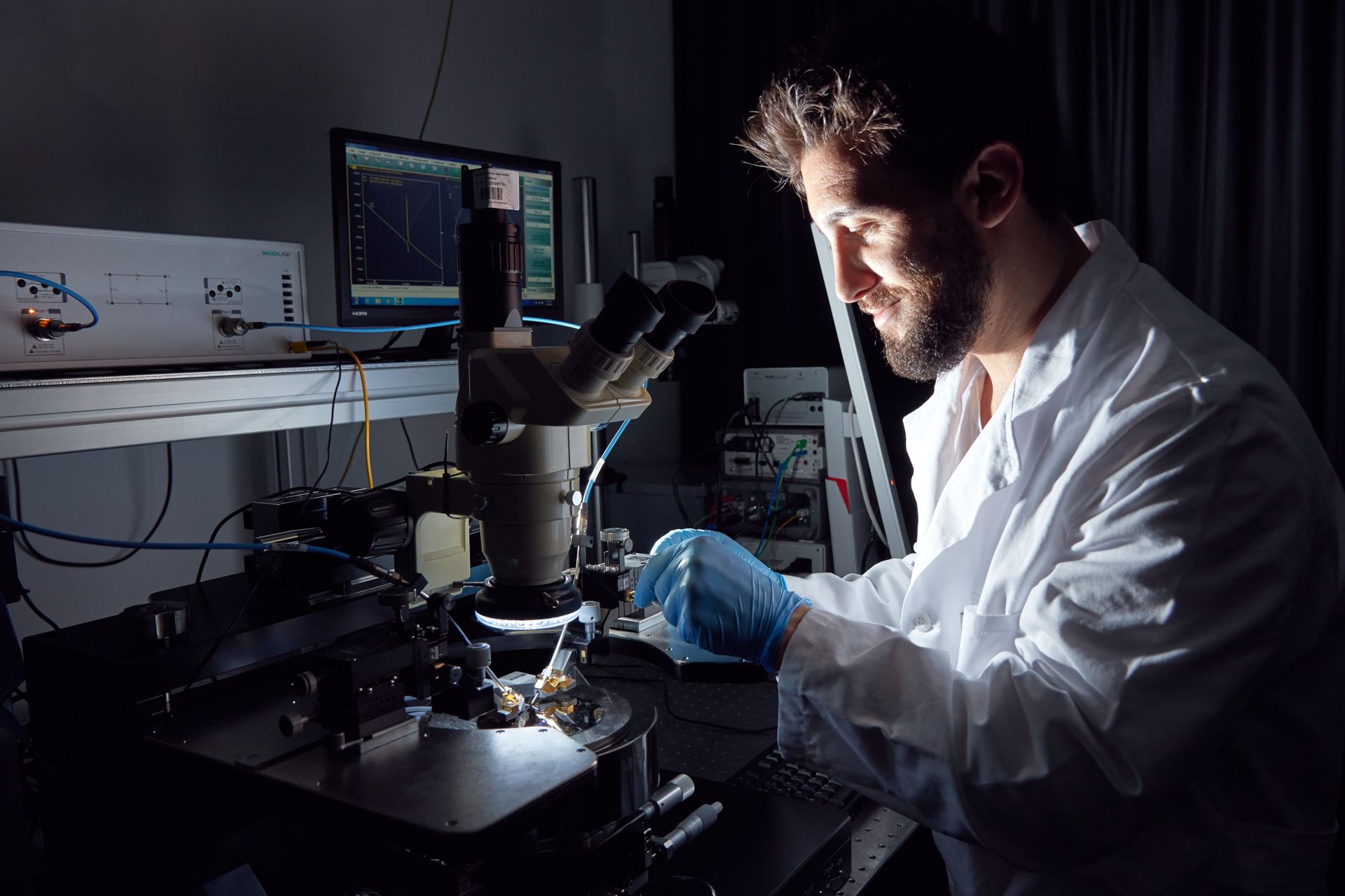
Portrait of a young male scientist at work.
© INATECH / Kilian Kreb
“Our idea is to use the anisotropic material properties of AlScN for acoustic filters.”

You recently applied for a patent, what is it about?

Anli — In our patent we were able to verify the c-axis orientation of a-plane AlScN and prove the optimal configuration for the highest electromechanical coupling by using experimental and theoretical methods.

Niclas — The a-axis orientation of the AlScN crystal gives rise to an enormous directional dependence within the wafer plane, which is crucial for the propagation of surface waves. Waves can thus be excited which would be difficult or impossible to observe in the c-axis orientation, e.g. shear waves. Due to the anisotropic material property of the crystal acoustic oscillations emerge that have an increased coupling coefficient and could be used for SAW filters or sensors.


What are the advantages of SAW filters based on AlScN?

Anli — Compared to the traditional material AlN, they can reach a higher electromechanical coupling, which means they have higher efficiency in transforming energy. Higher electromechanical coupling also leads to higher bandwidth. It also retains most advantages of AlN. This makes the material a promising material for next generation mobile communications.

Niclas — Our new thin films could cover additional frequency bands previously realized using bulk materials. As a result, the technology could lead to reduced production costs compared to conventional crystals. Our thin-film technology would require significantly less piezoelectric material and thus fewer raw materials such as lithium, niobium or tantalum, of which most bulk materials are made.

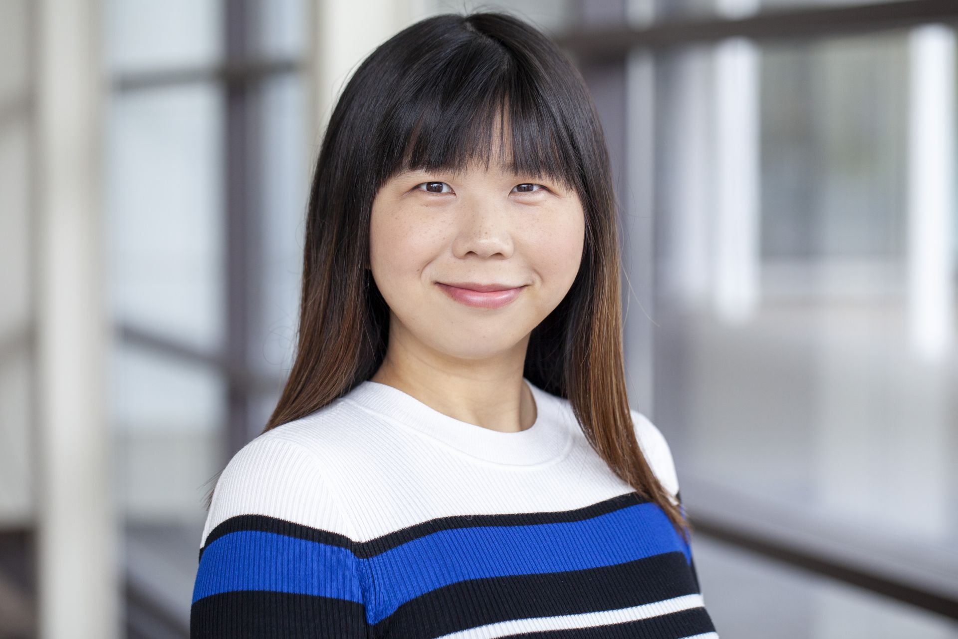
Porträt einer jungen Frau.
© Fraunhofer IAF
“For this purpose, we had to tilt the crystal axis of AlScN about 90°.”

How have you complemented each other in your research and what are your respective research areas?

Niclas — A whole team of researchers is involved in our research: scientific work is carried out from the development to the production of the components. I conduct research in the area of modeling. I use computer models to calculate the behavior of acoustic waves based on the anisotropic crystal properties. Using mathematical methods and special software, the acoustic waves in AlScN can be analyzed in detail. For this purpose, especially in the case of surface waves, the direction-dependent properties must be included in order to find, for example, suitable layer sequences and/or propagation directions.

Anli — I work in design, processing and characterization of components. In contrast to the simulation, we do not exactly know where the c-axis is in an experiment. I created a mask for fabricating SAW resonators with different propagation direction and different wavelengths, in order to test, how these parameters relate to the resonator performance. With my experimental approach, I could demonstrate the optimal configuration of SAW resonators based on a-plane AlScN which Niclas could then verify theoretically.


What has been the biggest challenge?

Niclas — For me, it was the experimental implementation. It always pleases me when theoretical concepts are confirmed in the form of a real experiment. I could always rely on the infrastructure and the cooperation between INATECH and Fraunhofer IAF.

Anli — A great challenge was to find a way to grow AlScN via sputtering with a quality that has not been reached before. Common approaches were limited in either the quality or the concentration of scandium. So we had to figure out how to grow it ourselves. By changing the underlying crystal structure to r-plane sapphire substrates, we managed to alter the formation of the AlScN crystal on top, which enabled us to grow a-plane AlScN with unprecedented qualities: We achieved the first documented growth of single crystalline a-plane AlScN with high Sc concentration.


Anli Ding started doing research at Fraunhofer IAF in the course of her master’s studies at IMTEK and is now continuing her work in the field of design, processing and characterization of components in her PhD.
Niclas Feil is researching for his PhD at INATECH and has an access contract to Fraunhofer IAF, which gives him full access to the institute's infrastructure.
Both are part of the AlScN research group at Fraunhofer IAF, which is led by Dr. Agne Zukauskaite and Dr. Maximilian Kessel. 

Further employees of Fraunhofer IAF in conversation


"The idea of building a computer from the tiniest particles has inspired me."

Kathrin König, PhD student quantum computing


"We are always there for our employees to offer advice and support."

Lena Breuer, Human Resources


"It's a real breakthrough for semiconductor technology."

Dr. Stefano Leone, Group leader epitaxy


All interviews

Here you can find all interviews with our colleagues.