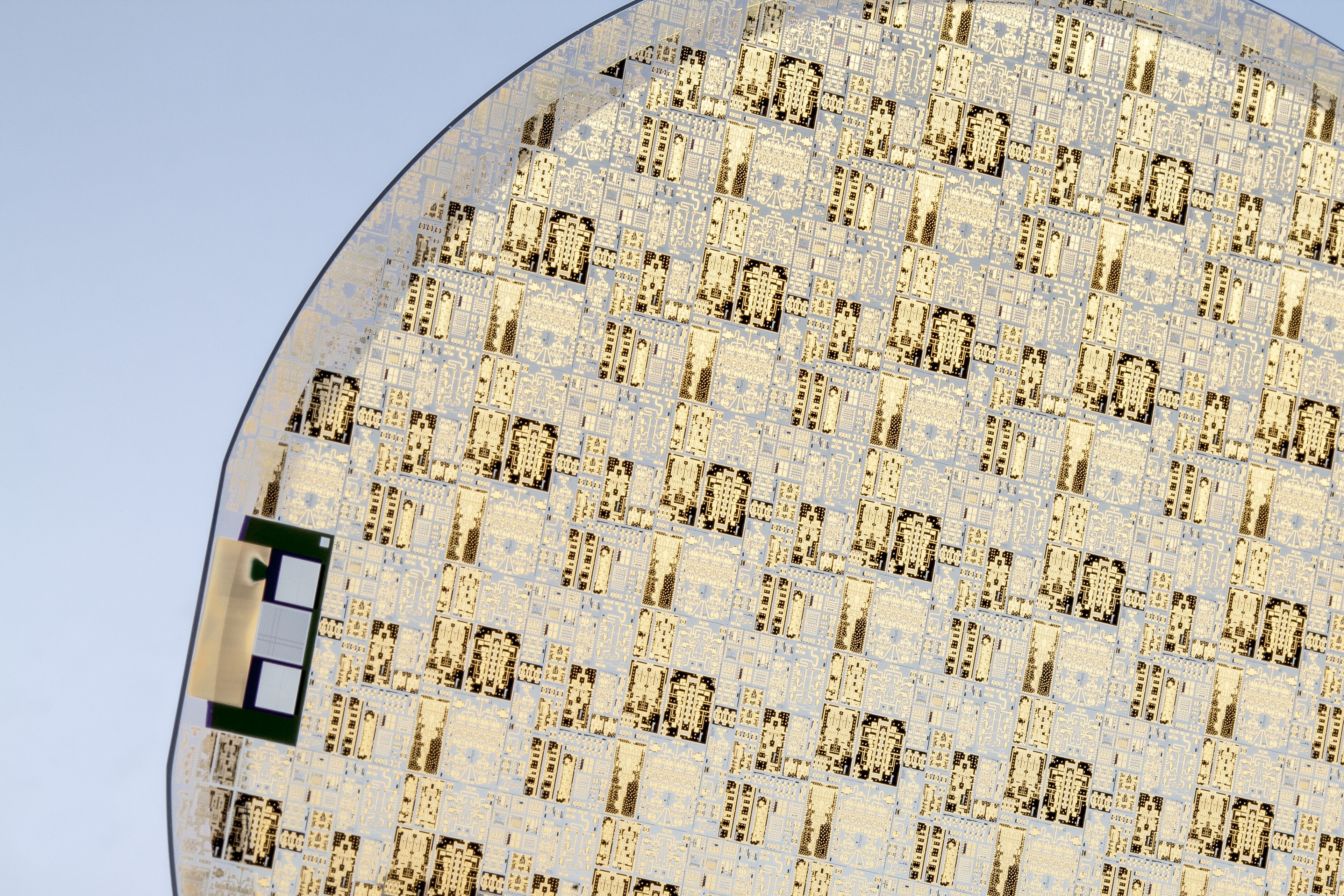
The aim of the CoGaN project is to investigate a compact design technique for integrated gallium nitride (GaN) power semiconductors in communication modules. Novel assembly concepts for GaN MMICs are investigated in this context. Due to their high power density, GaN MMICs offer extraordinary properties, but so far there is a lack of advanced assembly and interconnection concepts adapted to GaAs and silicon technology in order to open up new applications in a highly integrated and cost-effective way.
The project aims at developing new processes technology for GaN wafers, protective coatings and signal transmission. Aspects such as chip vitrification, bond wire-free HotVia technology, integrated and structured AuSn soldering and the air cavity package are also part of the research project.
 Fraunhofer Institute for Applied Solid State Physics IAF